
The SPP1305 is a P-channel logic enhancement mode power field effect transistor, produced using high cell density, DMOS trench technology. This high density process is especially tailored to minimize on-state resistance. These devices are particularly suited for low voltage applications such as cellular phone and notebook computer power management and other battery powered circuits where high-side switching, and low in-line power loss are needed in a very small outline surface mount package. Features: Super high density cell design for extremely low RDS(ON), Exceptional on-resistance and maximum DC current capability, SOT-323 (SC-70) package design.
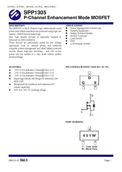
The SPP1305 is a P‑Channel logic enhancement mode MOSFET designed for high‑density, low‑voltage power‑management in notebook computers, cellular phones and other battery‑powered circuits. It offers very low on‑state resistance and high current capability in a compact SOT‑323 (SC‑70) surface‑mount package.
Key specifications include a drain‑source voltage rating of –20 V, gate‑source voltage of +12 V, typical on‑resistance of 0.28 Ω at VGS = ‑4.5 V, and continuous drain current up to –0.7 A at 70 °C. The datasheet provides detailed electrical characteristics, typical performance curves, and package dimensions.
| Drain‑Source Voltage (V_DSS) | -20 V |
|---|---|
| Gate‑Source Voltage (V_GSS) | +12 V |
| Continuous Drain Current (Ta=70 °C) | -0.7 A |
| Package Type | SOT‑323 (SC‑70) |
The SPP1305 is supplied in a SOT‑323 (SC‑70) surface‑mount package.
The device can tolerate a drain‑source voltage of –20 V and a gate‑source voltage of +12 V.