
SPP1413 is a P-channel logic enhancement mode power field effect transistor produced using high cell density, DMOS trench technology. This high density process is especially tailored to minimize on-state resistance. These devices are particularly suited for low voltage application such as cellular phone and notebook computer power management and other battery powered circuits where high-side switching, and low in-line power loss are needed in a very small outline surface mount package.
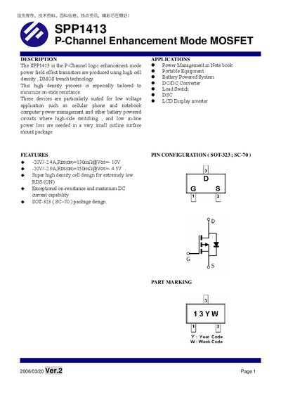
The SPP1413 P‑Channel MOSFET is designed for high‑density, low‑on‑resistance switching in battery‑powered devices such as notebooks and cellular phones. It uses DMOS trench technology to achieve a very small SOT‑323 (SC‑70) surface‑mount package.
Key electrical ratings include a -20 V drain‑source voltage, +12 V gate‑source voltage, up to 8 A pulsed drain current, and a typical on‑resistance of a few milliohms. The device is suitable for high‑side switching with minimal power loss and operates over a wide temperature range.
| Drain‑Source Voltage (V_DSS) | -20 V |
|---|---|
| Continuous Drain Current (Ta=70°C) | -2.0 A |
| Pulsed Drain Current (I_pM) | 8 A |
| Continuous Source Current (Diode Conduction) | -1.4 A |
| Thermal Resistance, Junction‑to‑Ambient | 105 °C/W |
The maximum drain‑source voltage is -20 V.
The device can handle up to -2.0 A continuous drain current at 70 °C.