
This document describes the features and applications of the SPP3407 P-Channel Enhancement Mode MOSFET product, which is suitable for low voltage applications such as cellphone, notebook computer power management, and other battery powered circuits.
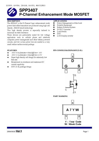
The SPP3407 is a P‑Channel logic‑level enhancement mode MOSFET designed for low‑voltage power‑management applications such as notebook computers, cellular phones and LCD inverter circuits. It features a high‑density DMOS trench structure that provides very low on‑resistance and minimal power loss in a compact SOT‑23‑3L package.
The document provides absolute maximum ratings, detailed electrical characteristics, typical performance curves, and mechanical dimensions of the SOT‑23‑3L package, enabling designers to evaluate the device for battery‑powered systems and DC‑DC converter load‑switch applications.
| Drain‑Source Voltage (V_DSS) | -30 V |
|---|---|
| Gate‑Source Voltage (V_GS) | +20 V |
| Continuous Drain Current (I_D) at 25 °C | -3.6 A |
| Pulsed Drain Current (I_DM) | -15 A |
| Operating Junction Temperature | 150 °C |
| Storage Temperature Range | -55 °C to 150 °C |
| Thermal Resistance, Junction‑to‑Ambient | 120 °C/W |
The device is rated for a maximum drain‑source voltage of -30 V.
Yes, it is specifically suited for low‑voltage LCD display inverter applications such as cellular phones and notebook computers.