
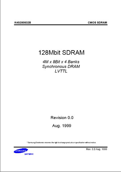
The K4S280832B is a 128 Mbit CMOS synchronous DRAM organized as 4 M × 8 bit with four banks. It complies with JEDEC 3.3 V standards and offers features such as auto‑refresh, programmable burst length, and selectable CAS latency.
The document lists absolute maximum ratings, recommended operating conditions (3.0‑3.6 V supply, -55 °C to +150 °C storage), pin configuration for a 54‑pin TSOP package, and detailed timing parameters for both DC and AC operation. IBIS specifications and a simplified truth table are also included.
| Capacity | 128 Mbit |
|---|---|
| Organization | 4 M × 8 bit × 4 banks |
| Supply voltage (VDD) | 3.0 V – 3.6 V (typ 3.3 V) |
| CAS latency | 2 or 3 clock cycles |
| Maximum operating frequency (CL‑3) | 133 MHz |
| Storage temperature range | -55 °C – +150 °C |
The recommended supply voltage is 3.3 V, with a range of 3.0 V to 3.6 V.
The device supports CAS latency of 2 or 3 clock cycles.
The CL‑3 version operates up to 133 MHz.
CLK is the system clock and is active on the positive‑going edge to sample all inputs.