
The TC7WBL125FK is a low-voltage dual bus switch manufactured by Toshiba. It has a working voltage of 2~3.6V, fast switching speed, low on-resistance, and good electrostatic discharge performance, making it suitable for analog signal transmission.
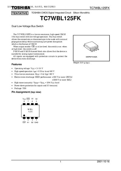
The TC7WBL125FK is a CMOS dual low‑voltage bus switch designed for fast, low‑power signal routing. It features an on‑resistance of about 5 Ω, propagation delay of 0.25 ns at 3 V, and robust electro‑static discharge protection suitable for analog signal transmission.
The device is supplied in an US8 (SSOP8‑P‑0.50A) package, weighs 0.01 g (typ.), and operates over a supply voltage range of –0.5 V to 7 V. Detailed electrical characteristics, maximum ratings, and package dimensions are provided for designers to ensure reliable integration in electronic systems.
| Operating voltage | 2 V ~ 3.6 V |
|---|---|
| Propagation delay (tpd) | 0.25 ns (max) @3 V |
| ESD protection | +200 V (JEITA), +2000 V (MIL) |
| Power supply voltage rating | -0.5 V ~ 7.0 V |
| Switch I/O current (Is) | 128 mA |
| Power dissipation (Pp) | 200 mW |
| Package type | US8 (SSOP8‑P‑0.50A) |
| Weight | 0.01 g (typ.) |
The device operates from 2 V to 3.6 V supply voltage.
It can withstand at least +200 V (JEITA) and +2000 V (MIL) ESD events.
The part is supplied in a US8 (SSOP8‑P‑0.50A) package.