
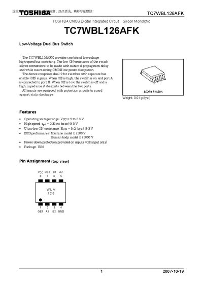
The TC7WBL126AFK is a low‑voltage dual bus switch that offers high‑speed switching with ultra‑low ON‑resistance, suitable for CMOS low‑power applications. It features dual 2‑bit switches with separate enable signals and built‑in ESD protection on inputs.
The document details the device's operating voltage range, propagation delay, ON‑resistance, package type, and environmental limits, along with absolute maximum ratings and recommended operating conditions for reliable integration in electronic systems.
| Operating voltage range | Vcc = 2 to 3.6 V |
|---|---|
| Propagation delay | tpd = 0.31 ns (max) @3 V |
| ON‑resistance | Ron = 5 Ω (typ) @3 V |
| ESD performance (Human body model) | +2000 V |
| Weight | 0.01 g (typ.) |
| Power dissipation | 200 mW |
| Switch I/O current | Is 128 mA |
| Storage temperature | -65~150 °C |
The device operates with a supply voltage Vcc from 2 V to 3.6 V.
The typical ON‑resistance is 5 Ω at a 3 V supply.
The power‑supply voltage may not exceed –0.5 V to 4.6 V.