
The TC7WBL125FK is a low-voltage dual bus switch from Toshiba. It operates at a voltage range of 2~3.6V and has a very fast switching speed of 0.25ns. The switching resistance is also very low, only 5Ω. The chip also features ESD static discharge protection, high noise immunity, and is suitable for analog signal transmission.
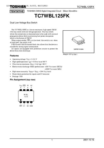
The TC7WBL125FK is a dual low‑voltage bus switch offering low on‑resistance, high‑speed operation and ESD protection. It is designed for analog signal transmission and includes input protection circuits.
The document provides maximum ratings, electrical characteristics, package dimensions and usage restrictions, helping designers integrate the device safely into electronic systems.
| Operating voltage (Voc) | 2 ~ 3.6 V |
|---|---|
| Propagation delay (tpd) | 0.25 ns (max) @3 V |
| On‑resistance (RON) | 5 Ω (typ.) @3 V |
| ESD performance | +200 V (JEITA), +2000 V (MIL) |
| Power supply voltage range | -0.5 ~ 7.0 V |
| Switch I/O current (Is) | 128 mA |
| Power dissipation (Pp) | 200 mW |
| Package | SSOP8‑P‑0.50A (US8) |
| Weight | 0.01 g (typ.) |
The device operates from 2.0 V to 3.6 V.
The propagation delay is up to 0.25 ns at a 3 V supply.
It can withstand at least +200 V (JEITA) and +2000 V (MIL) electro‑static discharge.