
TC7WBL125AFK is a low-voltage dual bus switch produced by Toshiba. It operates at a voltage range of 2 to 3.6 V, with a switching time of 0.31 ns and a switching resistance of 5 ohms. It supports the ESD protection of ±2000 V and US8 packaging.
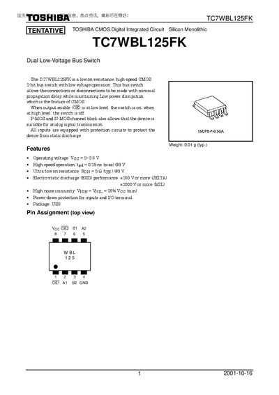
The TC7WBL125FK is a dual low‑voltage bus switch from Toshiba, offering low on‑resistance and high‑speed operation for analog and digital signal routing. It features CMOS technology with protection circuits on all inputs and a compact SSOP8 package.
Key specifications include an operating voltage of 2‑3.6 V, propagation delay of 0.25 ns, typical on‑resistance of 5 Ω, and ESD ratings of +200 V (JEITA) and +2000 V (MIL). The device is intended for general electronics applications and includes detailed maximum ratings, recommended operating conditions, and package dimensions.
| Operating voltage (Voc) | 2 V ~ 3.6 V |
|---|---|
| Propagation delay (tpd) | 0.25 ns (max) @3 V |
| On‑resistance (RON) | 5 Ω (typ.) @3 V |
| ESD performance | +200 V (JEITA), +2000 V (MIL) |
| Power dissipation (Pp) | 200 mW |
| Switch I/O current (Is) | 128 mA |
| Package type | US8 (SSOP8‑P‑0.50A) |
| Weight | 0.01 g (typ.) |
The device operates from 2 V to 3.6 V.
The typical on‑resistance is 5 Ω at 3 V.
It can withstand +200 V (JEITA) and +2000 V (MIL) ESD events.
The part is supplied in a US8 (SSOP8‑P‑0.50A) package.