
TC7WBL125AFK is a low-voltage dual bus switch with features such as low ON-resistance, high speed, and low power dissipation.
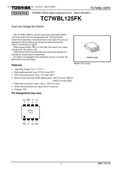
The TC7WBL125FK is a CMOS dual 2‑bit bus switch designed for low‑voltage operation. It provides ultra‑low on‑resistance (≈5 Ω typical) and a propagation delay as fast as 0.25 ns at 3 V, while maintaining low power dissipation. The device includes protection circuits on all inputs and supports both P‑MOS and N‑MOS channel blocks for analog signal transmission.
Typical applications include general electronics such as computers, office equipment, measuring devices, industrial robotics and domestic appliances. Users should observe the recommended operating voltage ranges and handling guidelines to ensure reliable performance and safety.
| Operating voltage (VCC) | 2~3.6 V |
|---|---|
| Propagation delay (tpd) | 0.25 ns (max) @3 V |
| On‑resistance (RON) | 5 Ω (typ.) @3 V |
| ESD performance | +200 V (JEITA), +2000 V (MIL) |
| Switch I/O current (Is) | 128 mA |
| Power dissipation (Pp) | 200 mW |
| Storage temperature | -65~150 °C |
The typical on‑resistance is about 5 Ω at 3 V.
It has a propagation delay of up to 0.25 ns when operated at 3 V.
The power supply voltage should be between 2.0 V and 3.6 V, and control pins operate from 0 V to 5.5 V.