
TC7WBD126FK is a low on-resistance, high-speed CMOS 2-bit bus switch with low power dissipation. It allows connections or disconnections to be made with minimal propagation delay. When the output enable (OE) is high, the switch is on; when it is low, the switch is off. The device also has an internal diode that enables the shift of signal level from 5V to 3.3V.
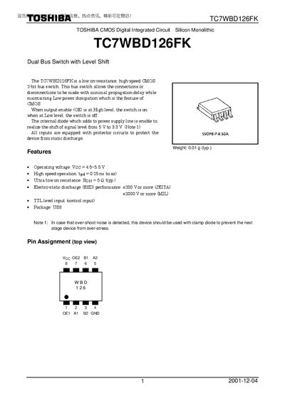
The TC7WBD126FK is a low on‑resistance, high‑speed CMOS dual‑bus switch with level‑shift capability, allowing fast connection and disconnection of signals while maintaining low power dissipation. It operates with a supply voltage of 4.5 V to 5.5 V and includes built‑in protection against static discharge.
The datasheet details the device's electrical parameters such as propagation delay, on‑resistance, ESD performance, and power dissipation, as well as mechanical information like package dimensions and recommended operating conditions. It also outlines usage restrictions and reliability guidelines for designers.
| Operating voltage (Voc) | 4.5~5.5 V |
|---|---|
| Propagation delay (tpd) | 0.25 ns (max) |
| ESD performance | +200 V (JEITA), +2000 V (MIL) |
| Continuous channel current (Is) | 128 mA |
| Power dissipation (Pp) | 200 mW |
| Storage temperature (Tsig) | -65~150 °C |
| Operating temperature (Topr) | -40~85 °C |
The device operates with a supply voltage (Voc) from 4.5 V to 5.5 V.
The recommended supply voltage (Voc) is 4.5 V to 5.5 V.