
The TC7WBD126FK is a low on-resistance, high-speed CMOS 2-bit bus switch. It has the low power dissipation feature of CMOS. When the output enable (OE) is high, the switch is on; when it is low, the switch is off. The internal diode allows the signal level to shift from 5V to 3.3V.
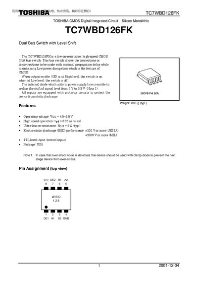
The TC7WBD126FK is a CMOS dual‑bus switch that provides low on‑resistance and high‑speed operation while shifting signal levels from 5 V to 3.3 V. It features protected inputs, ESD robustness, and a compact SSOP8‑P‑0.50A package.
Typical specifications include a 4.5‑5.5 V operating voltage, 0.25 ns propagation delay, 5 Ω typical on‑resistance, and a power dissipation of 200 mW. The device is rated for continuous channel current of 128 mA and operates over a storage temperature range of –65 °C to 150 °C.
| Operating voltage (Voc) | 4.5 ~ 5.5 V |
|---|---|
| Propagation delay (tpLH) | 0.25 ns (max) |
| On‑resistance (Ron) | 5 Ω (typ.) |
| ESD performance | +200 V (JEITA), +2000 V (MIL) |
| Package | SSOP8‑P‑0.50A |
| Power dissipation | 200 mW |
| Continuous channel current (Is) | 128 mA |
| Storage temperature | -65 °C ~ 150 °C |
The device operates with a supply voltage (Voc) of 4.5 V to 5.5 V.
The typical on‑resistance is 5 Ω.
It is supplied in an SSOP8‑P‑0.50A (US8) package.
It meets +200 V (JEITA) and +2000 V (MIL) ESD performance.