
This document describes the TC7WG125FU/FK model of TOSHIBA CMOS digital integrated circuit silicon monolithic, including its features such as high-level output current, high-speed operation, operating voltage range, etc.
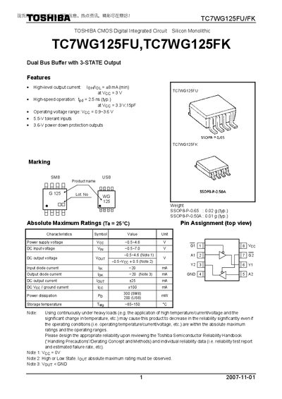
The TC7WG125FU/FK is a dual‑bus buffer with 3‑state output designed for CMOS digital integrated circuits. It offers high‑level output current of up to +8 mA and operates over a wide voltage range, making it suitable for general electronics applications such as computers, office equipment, and industrial robotics.
Key specifications include an operating voltage range of 0.9 V to 3.6 V, typical propagation delay of 2.5 ns, power dissipation of 200 mW, and a compact SSOP8 package weighing as little as 0.01 g. The document also outlines reliability notes, package dimensions, and restrictions on use in safety‑critical systems.
| High‑level output current | +8 mA (min) |
|---|---|
| Operating voltage range | 0.9 V ~ 3.6 V |
| Propagation delay (tpd) | 2.5 ns (typ.) |
| Power dissipation | 200 mW |
| Storage temperature | -65 °C ~ 150 °C |
| Package weight (SSOP8‑P‑0.65) | 0.02 g (typ.) |
| Package dimensions (SSOP8‑P‑0.65) | 2.94 mm × 0.65 mm × 0.65 mm |
The device operates from 0.9 V to 3.6 V.
The maximum power dissipation is 200 mW.
The SSOP8‑P‑0.65 package measures 2.94 mm × 0.65 mm × 0.65 mm.
Yes, the device must not be used in equipment where failure could cause loss of life or injury, such as medical, aerospace, or safety‑critical systems.