
This document provides information about the PC board footprint dimensions of the SOT713-1_fp product from Koninklijke Philips Electronics N.V. It includes solder land dimensions, solder paste occupied area, and footprint information for reflow soldering of the TFBGA204 package.
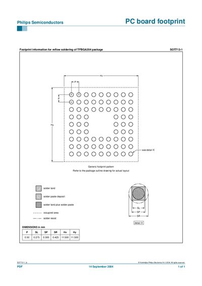
The document describes the PCB footprint for the Philips SOT713-1 component, intended for reflow soldering of the TFBGA204 package. It includes a generic footprint pattern and references to the package outline drawing for the exact layout.
Dimensions are given in millimetres for pad size, solder paste deposit, and overall board area, and the manual is copyrighted by Koninklijke Philips Electronics N.V. (2004).
| Pad width (P) | 0.50 mm |
|---|---|
| Solder land width (SL) | 0.275 mm |
| Solder paste width (sP) | 0.300 mm |
| Solder resist width (SR) | 0.425 mm |
| Horizontal dimension (Hx) | 11.500 mm |
| Vertical dimension (Hy) | 11.500 mm |
It is for the TFBGA204 package.
Refer to the package outline drawing for the actual layout.