
This document describes how to use the demonstration board DEMO8766G for the analog-to-digital converter ADC1002S020. The features of the demo board include a 2Vpp input signal range, a single TTL-CMOS clock signal, and a 3.3V power supply.
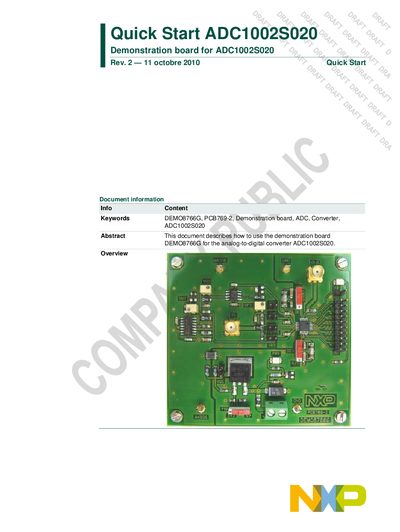
This guide explains how to use the ADC1002S020 demo board and the optional HSDC‑EXTMOD01/DB acquisition module. It describes the board’s power supply, voltage adjustments, input and output signal connections, and the required synchronization of the input signal and clock.
The document also provides step‑by‑step instructions for installing the USB Configurator software used to control the HSDC extension module, as well as hardware initialization procedures and a brief overview of measurement set‑up and data acquisition features.
| Power supply voltage | 12 V |
|---|---|
| Power supply current rating | 50 mA |
| Full‑scale input range | 1.6 V to 2.4 V |
| TOP reference (typical) | 3.3 V |
| BOT reference (typical) | 1.2 V |
| Analog input connector impedance | 50 Ω (matching) |
| Clock input connector impedance | 50 Ω (matching) |
| Digital output connector | Array connector (DO to D9) |
The board is powered with a single 12 V power supply, and a regulator on the board provides the required 3.3 V and other internal voltages.
Use the VRT, VRB, and OFS trimmers to set the TOP reference, BOT reference, and offset, allowing the full‑scale input to be set between 1.6 V and 2.4 V.
Run the installer (CDM 2.04.16.exe) from the CD, follow the wizard by clicking Next, choose the installation folder, and confirm the installation to complete the setup.
The TOP reference is typically 3.3 V and the BOT reference is typically 1.2 V.