
This document is about SOT1063-1 PCB footprint information
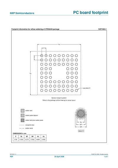
This document supplies the PCB footprint information required for reflow soldering of the NXP SOT1063-1 component, which uses a VFBGA48 package. It lists the solder land sizes, paste deposit guidelines, and occupied area definitions.
The layout dimensions are given in millimetres, with pad pitches of 4.400 mm in both X and Y directions. For the exact outline, refer to the package outline drawing referenced in the manual.
It uses a VFBGA48 package.
Refer to the package outline drawing for the actual layout.
The document is dated 29 April 2008.