
This datasheet provides information on the maximum ratings, thermal characteristics, ESD protection characteristics and moisture sensitivity level of MRFG35010ANT1.
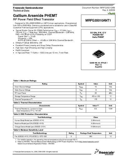
The MRFG35010ANT1 is a Gallium Arsenide PHEMT RF power field‑effect transistor designed for WLL/MMDS/BWA or UMTS driver applications. It operates from 500 MHz to 5 GHz, delivering up to 9 W output power at 3.5 GHz with high gain, efficiency, and linearity.
The data sheet provides maximum ratings, thermal and ESD characteristics, electrical parameters, and typical performance graphs. It also includes a 3.5 GHz test circuit schematic, component values, and S‑parameter tables for design reference.
| Drain‑Source Voltage (Voss) | 15 V |
|---|---|
| Gate‑Source Voltage (Ves) | -5 V |
| RF Input Power (Pin) | 33 dBm |
| Storage Temperature Range | -65 °C to +150 °C |
| Power Gain | 10 dB |
| Drain Efficiency | 25 % |
| Adjacent Channel Power Ratio (ACPR) | -43 dBc @ 5 MHz offset |
| RoHS Compliance | Yes |
The maximum drain‑source voltage is 15 V.
It is characterized from 500 MHz to 5 GHz.
Yes, the device is RoHS compliant.
The recommended storage temperature range is -65 °C to +150 °C.