
MRF5S9100NR1/NBR1 is a RF power field effect transistor designed for broadband commercial and industrial applications with frequencies up to 1000 MHz. It offers high gain and broadband performance, making it ideal for large-signal, common-source amplifier applications in 26 volt base station equipment. The product is capable of handling 10:1 VSWR and operates at a maximum voltage of 32 VDD.
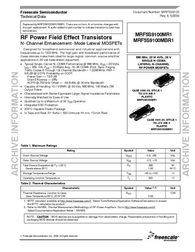
This document provides the technical specifications, electrical characteristics, and mechanical dimensions for the Freescale MRF5S9100MR1 and MRF5S9100MBR1 N‑channel lateral MOSFETs. The devices are designed for broadband commercial and industrial applications up to 1000 MHz, offering high gain and efficiency for large‑signal amplifier use.
Key sections include maximum ratings, thermal characteristics, ESD protection, moisture sensitivity, typical performance graphs, and detailed package drawings. The data sheet also contains a test‑circuit schematic and component list for evaluation.
| Drain‑Source Voltage (Voss) | 0.5 V to +68 V |
|---|---|
| Gate‑Source Voltage (Ves) | -0.5 V to +15 V |
| Total Device Dissipation | 336 W |
| Storage Temperature Range | -65 °C to +150 °C |
| Operating Junction Temperature | 200 °C |
| Power Gain | 19.5 dB |
| Drain Efficiency | 28 % |
| Adjacent Channel Power Ratio (ACPR) | -46.8 dBc |
The device can handle a drain‑source voltage from 0.5 V up to +68 V.
MOS devices are susceptible to electrostatic discharge, so reasonable ESD precautions should be observed during handling and packaging.
Typical power gain is 19.5 dB.