
MRF9135LR3 and MRF9135LSR3 are RF power field effect transistors manufactured by Freescale Semiconductor. They are designed for broadband commercial and industrial applications with frequencies from 865 to 895 MHz. These devices have high gain and broadband performance, making them ideal for large-signal, common-source amplifier applications in 26 volt base station equipment. Under typical N-CDMA performance at 880 MHz, 26 volts, and IDQ = 1100 mA, they have an output power of 25 watts, power gain of 17.8 dB, efficiency of 25%, and adjacent channel power of -47 dBc at 750 kHz with 30 kHz bandwidth. These devices are capable of handling 10:1 VSWR, with 135 watts CW output power at 26 Vdc and 880 MHz. They feature internally matched for ease of use, high gain, high efficiency, and high linearity. They also have integrated ESD protection, designed for maximum gain and insertion phase flatness, excellent thermal stability, characterized with series equivalent large-signal impedance parameters, low gold plating thickness on leads (40μ″ nominal), and RoHS compliant. They are supplied in tape and reel form.
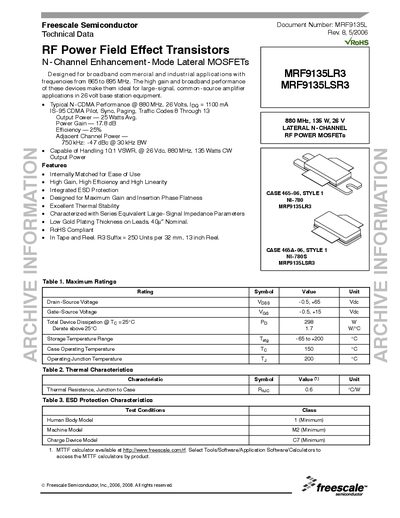
This datasheet provides the electrical, thermal and mechanical specifications for the Freescale MRF9135LR3 and MRF9135LSR3 N‑channel lateral MOSFETs, designed for broadband commercial and industrial RF applications from 865 MHz to 895 MHz. It includes typical performance figures such as 25 W average output power, 17.8 dB gain and 25 % efficiency at 880 MHz.
The document also lists maximum ratings, package dimensions, test‑circuit schematics, and contact information for Freescale Semiconductor support centers worldwide.
| Output Power (Avg) | 25 W |
|---|---|
| Power Gain | 17.8 dB |
| Efficiency | 25 % |
| Drain‑Source Voltage (Voss) | -0.5 to +65 V |
| Gate‑Source Voltage (Ves) | -0.5 to +15 V |
| Total Device Dissipation | 298 W |
| Thermal Resistance, Junction‑to‑Case (Rjc) | 0.6 °C/W |
| Package Style | CASE 465‑06, STYLE 1 |
| Package Dimension A (length) | 1.335 – 1.345 in |
The device can deliver up to 25 W average output power.
Drain‑source voltage is rated from –0.5 V to +65 V, and gate‑source voltage from –0.5 V to +15 V.
The junction‑to‑case thermal resistance is 0.6 °C/W.
They are supplied in CASE 465‑06, STYLE 1 packages.