
MRF5S9101MR1/MBR1 is a RF Power Field Effect Transistors N-Channel Enhancement-Mode Lateral MOSFETs produced by Freescale Semiconductor. It is designed for GSM and GSM EDGE base station applications with frequencies from 869 to 960 MHz and the maximum output power is 100 watts.
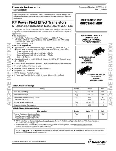
This datasheet provides detailed specifications for the Freescale MRF5S9101MR1 and MRF5S9101MBR1 N‑channel lateral MOSFETs, designed for GSM and GSM‑EDGE base‑station applications from 869 MHz to 960 MHz. It includes typical performance figures such as 100 W CW output at 26 V for GSM and 50 W average at 28 V for EDGE, along with power gain and efficiency data.
The document lists maximum ratings, thermal characteristics, electrical parameters, ESD protection, moisture‑sensitivity level, and mechanical dimensions. A 900 MHz test circuit schematic and component layout are provided, as well as contact information for Freescale technical support worldwide.
| Drain‑Source Voltage (VDS) | -0.5 V to +68 V |
|---|---|
| Gate‑Source Voltage (VGS) | -0.5 V to +15 V |
| Total Device Dissipation | 427 W @ 25 °C |
| Storage Temperature Range | -65 °C to +150 °C |
| Operating Junction Temperature | 200 °C |
| Drain‑Source On‑Voltage (VDS(on)) | 0.241 V typical |
| Gate Threshold Voltage (Vth) | 2.8 V to 3.5 V |
| Output Capacitance (Coss) | 70 pF |
| Power Gain (GSM) | 17.5 dB typical |
| Drain Efficiency (GSM) | 60 % typical |
| Package Style | CASE 1486-03, STYLE 1 TO-270 WB-4 PLASTIC |
| Units per Reel (R1 suffix) | 500 units per 44 mm (13 in) reel |
The device can handle a drain‑source voltage from –0.5 V up to +68 V.
It is supplied in a CASE 1486‑03, STYLE 1 TO‑270 WB‑4 plastic package.
Typical power gain is 17.5 dB for GSM operation.
The R1 suffix indicates 500 units per 44 mm (13 in) reel.