
This data sheet provides the characteristics parameters of MRF9060NR1 RF power field effect transistor, such as maximum ratings, typical parameters, temperature characteristics, etc. This device is suitable for large-signal, common-source amplifier applications in 26V base station equipment.
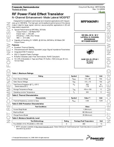
The MRF9060NR1 is a lateral N‑channel enhancement‑mode MOSFET designed for broadband commercial and industrial RF applications up to 1000 MHz. It provides 60 W peak‑envelope power at 945 MHz, 26 V bias, with 18 dB gain and 40 % efficiency in two‑tone tests.
The device is supplied in a TO‑270‑2 plastic package (available in tape and reel) and is RoHS‑compliant. Key electrical limits include a 65 V drain‑source rating, 15 V gate‑source rating, and a maximum dissipation of 223 W at 25 °C. Thermal resistance from junction to case is 0.56 °C/W, and the part can operate up to a junction temperature of 200 °C.
| Drain‑Source Voltage (Vdss) | 65 V |
|---|---|
| Gate‑Source Voltage (Vgss) | 15 V |
| Total Device Dissipation | 223 W @ 25 °C |
| Operating Junction Temperature | 200 °C |
| Thermal Resistance, Junction‑to‑Case | 0.56 °C/W |
| Maximum Output Power | 60 W PEP at 945 MHz, 26 V |
| Power Gain | 18 dB |
| Efficiency (Two‑Tone) | 40 % |
| Intermodulation Distortion (IMD) | -31.5 dBc |
| Package Type | TO‑270‑2 plastic, tape & reel |
| RoHS Compliance | Yes (lead‑free) |
The device can deliver up to 60 W peak‑envelope power at 945 MHz with a 26 V bias.
The drain‑source voltage rating is 65 V and the gate‑source rating is 15 V.
It is supplied in a TO‑270‑2 plastic package, available in tape and reel form.
Yes, the device is RoHS‑compliant and uses lead‑free terminations.