
MRF18090AR3 RF Power Field Effect Transistor is a N-Channel Enhancement-Mode Lateral MOSFET from Freescale Semiconductor (Freescale Semiconductor) suitable for applications in the frequency range of 1800 to 2000 MHz for GSM and GSM EDGE base stations.
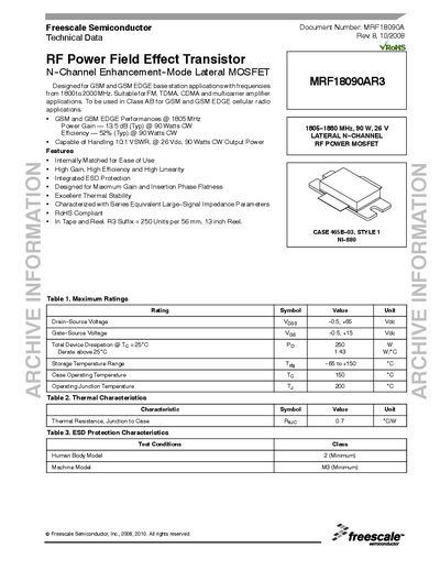
The MRF18090AR3 RF Power Field Effect Transistor is a N‑channel enhancement‑mode lateral MOSFET designed for GSM, GSM‑EDGE, FM, TDMA, CDMA and multicarrier amplifier applications in the 1800‑2000 MHz band. It is intended for use in Class AB base‑station power amplifiers and is supplied in a 465B‑03 package.
Key performance figures include a typical power gain of 13.5 dB at 90 W CW, 52 % efficiency at the same output level, and the ability to handle a 10:1 VSWR. The device is RoHS compliant, internally matched for ease of use, and features integrated ESD protection and high linearity.
| Drain‑Source Voltage (Voss) | +65 V |
|---|---|
| Gate‑Source Voltage (Vgs) | +415 V |
| Total Device Dissipation | 250 W |
| Operating Junction Temperature (Tj) | 200 °C |
| Power Gain (typical) | 13.5 dB @ 90 W CW |
| Efficiency (typical) | 52 % @ 90 W CW |
| Frequency Range | 1800‑2000 MHz |
| Maximum Output Power | 90 W CW |
| Package | CASE 465B‑03, STYLE 1 |
The device is rated for a maximum drain‑source voltage of +65 V.
At 90 W continuous wave output, the typical power gain is 13.5 dB.
The typical efficiency at 90 W CW is 52 %.
The transistor can operate up to a junction temperature of 200 °C.