
MRFE6S9130HR3 / MRFE6S9130HSR3 is a RF power field effect transistor, suitable for N-CDMA and GSM base station applications with frequencies from 865 to 960 MHz.
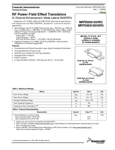
This datasheet provides the electrical, thermal and mechanical specifications for the N‑channel lateral MOSFETs MRFE6S9130HR3 and MRFE6S9130HSR3, designed for N‑CDMA, GSM and GSM‑EDGE base‑station applications from 865 MHz to 960 MHz. It includes typical performance figures such as power gain, drain efficiency and ACPR, as well as maximum ratings and test‑circuit details.
The document also lists recommended PCB material, ESD protection characteristics, and references to application notes and engineering bulletins for further design guidance. Revision history and contact information for Freescale Semiconductor are included at the end.
| Drain‑Source Voltage (Voss) | -0.5 V to +66 V |
|---|---|
| Gate‑Source Voltage (Ves) | -0.5 V to +12 V |
| Storage Temperature Range | -65 °C to +150 °C |
| Maximum Junction Temperature (Ty) | 225 °C |
| Power Gain | 19.2 dB (typical) |
| Drain Efficiency | 30.5 % |
| ACPR @ 750 kHz Offset | -47.6 dBc |
| Maximum Continuous Output Power | 27 W Avg. (28 Vpp, 950 mA) |
| ESD Protection (Human Body Model) | ≥ 1 A |
The device can tolerate a drain‑source voltage from –0.5 V up to +66 V.
Typical power gain is 19.2 dB.
Typical drain efficiency is 30.5 %.
Human Body Model protection is at least 1 A, Machine Model at least A, and Charge Device Model at least 1 V.