
This document describes the features and characteristics of MRF5S21090HR3 and MRF5S21090HSR3 RF power field effect transistors. They are N-channel enhancement-mode lateral MOSFETs designed for W-CDMA base station applications with frequencies from 2110 to 2170 MHz. They are suitable for TDMA, CDMA, and multicarrier amplifier applications. They can be used in Class AB for PCN-PCS/cellular radio and WLL applications. The document also provides typical values for 2-carrier W-CDMA performance. The products feature high power gain, low thermal resistance, integrated ESD protection, RoHS compliance, etc.
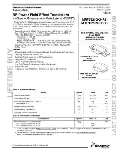
The MRF5S21090HR3 is an N‑channel enhancement‑mode lateral MOSFET designed for W‑CDMA base‑station applications covering 2110‑2170 MHz. It is suitable for TDMA, CDMA and multicarrier amplifier designs and can handle up to 10:1 VSWR at 28 Vde.
Key performance figures include a typical output power of 19 W average, 14.5 dB power gain, 26 % drain efficiency, and a maximum drain‑source voltage of +65 Vde. The device is internally matched, RoHS compliant, and offered in a CASE 465‑06, STYLE 1 package with tape‑and‑reel packaging.
| Drain‑Source Voltage (Voss) | -0.5, +65 Vde |
|---|---|
| Gate‑Source Voltage (Ves) | -0.5, +15 Vde |
| Total Device Dissipation (Pp) | 269 W |
| Power Gain | 14.5 dB |
| Drain Efficiency | 26 % |
| Typical Output Power | 19 W Avg. |
| Operating Frequency Range | 2110‑2170 MHz |
| Package Type | CASE 465‑06, STYLE 1 |
| RoHS Compliance | Yes |
The device is rated for a drain‑source voltage from –0.5 V to +65 Vde.
Yes, the datasheet notes that the part is RoHS compliant.
It is intended for W‑CDMA base‑station use from 2110 MHz to 2170 MHz.