
The PI6C2404A-1 is a PLL-based, zero-delay buffer, with the ability to distribute four outputs of up to 133 MHz at 3.3V. Two banks of two outputs exist, OUTA[1–2] and OUTB[1–2]. An external feedback pin is used to synchronize the outputs to the input; the relationship between loading of this signal and the other outputs determines the input-output delay. The PI6C2404A-1 is characterized for both commercial and industrial operation.
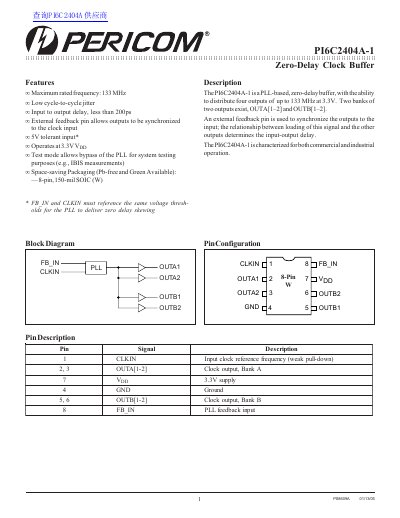
This document is a technical datasheet for the Pericom PI6C2404A-1 Zero-Delay Clock Buffer. The device is a PLL-based component designed to distribute four outputs of up to 133 MHz at 3.3V with low cycle-to-cycle jitter and input-to-output delay less than 200ps.
| Maximum rated frequency | 133 MHz |
|---|---|
| Supply Voltage | 3.0V to 3.6V |
| Operating Temperature (Commercial) | 0°C to +70°C |
| Operating Temperature (Industrial) | -40°C to +85°C |
| Output Frequency | 10 MHz to 133 MHz |
| Package Type | 8-pin, 150-mil SOIC (W) |
The PI6C2404A-1 has a maximum rated frequency of 133 MHz.
The input to output delay is less than 200ps.