
The PI6C2510-133 is a low-noise phase-locked loop clock driver, distributing high-frequency clock signals for SDRAM and server applications. It features operating frequency up to 150 MHz, low-noise phase-locked loop clock distribution that meets 133 MHz Registered DIMM Synchronous DRAM modules for server/workstation/PC applications, allows clock input to have spread spectrum modulation for EMI reduction, zero input-to-output delay, low jitter, and on-chip phase-locked loop.
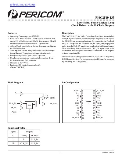
The PI6C2510-133 is a low-skew, low-jitter phase-locked loop (PLL) clock driver that distributes high-frequency clock signals for SDRAM and server applications. It features zero input-to-output delay when the feedback output is connected to the feedback input, allowing one clock input to drive ten outputs with an enable function.
The device operates at a supply voltage of 3.0V to 3.6V and supports operating frequencies up to 150 MHz. It includes on-chip series damping resistors for low noise and EMI reduction and is available in a 24-pin TSSOP package.
| Operating Frequency | up to 150 MHz |
|---|---|
| Supply Voltage | 3.0V to 3.6V |
| Number of Outputs | 10 Clock Outputs |
| Package Type | 24-pin TSSOP (L) |
| Cycle-to-Cycle Jitter | +75ps max. |
The device supports an operating frequency up to 150 MHz.
By connecting the feedback FB OUT output to the feedback FB IN input, the propagation delay from CLK_IN to any clock output will be nearly zero.
Yes, for test purposes, the PLL can be bypassed by strapping AVcc to ground.