
CDC319 is a 1-to-10 clock buffer that supports SDRAM clock buffering applications. The output skew (tsk(o)) is less than 250 ps, and the pulse skew (tsk(p)) is less than 500 ps. It supports up to two unbuffered SDRAM DIMMs (Dual Inline Memory Modules). The I2C serial interface provides individual enable control for each output. It operates at 3.3V. Distributed VCC and ground pins reduce switching noise. The ESD protection voltage exceeds 2000V, meeting the requirements of MIL-STD-883 Method 3015. It is packaged in a 28-pin Shrink Small Outline (DB) package.
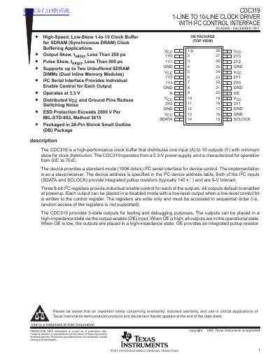
The CDC319 is a high-performance clock buffer designed to distribute one input clock signal to ten outputs with minimum skew. It operates from a 3.3-V power supply and is characterized for temperatures from 0°C to 70°C. The device features a standard I2C serial interface for individual enable control of each output, allowing configuration via three 8-bit registers. It supports up to two unbuffered SDRAM DIMMs and includes ESD protection exceeding 2000 V.
| Supply Voltage | 3.3 V |
|---|---|
| Operating Temperature | 0°C to 70°C |
| Output Skew | Less Than 250 ps |
| Pulse Skew | Less Than 500 ps |
| Package Type | 28-Pin DB Package |
The output skew is less than 250 ps.
The device distributes one input to 10 outputs.
The device operates from a 3.3-V power supply.