
This manual introduces the use of Power56 MOSFET, including mounting techniques and circuit design. The MOSFET has the characteristics of miniaturization, high performance and low power consumption.
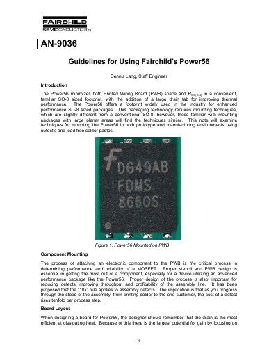
This document provides guidelines for using Fairchild Semiconductor's Power56 MOSFET, which features a large drain tab for improved thermal performance in an SO-8 footprint. It details specific mounting techniques for both prototype and manufacturing environments, focusing on the critical process of attaching the component to the Printed Wiring Board (PWB). Key areas of focus include board layout optimization for heat dissipation and specific recommendations for via placement to enhance thermal performance without compromising manufacturability.
The guide covers the solder process in detail, including stencil design, solder paste selection (eutectic and lead-free), and reflow profiles. It addresses common issues such as exposed copper on lead ends and solder fillet formation. Additionally, the document offers instructions for production assembly using standard pick and place equipment, as well as specific methods for rework and prototype mounting using hot air guns.
| Maximum seating plane tolerance | 0.06mm |
|---|---|
| Peak temperature tested | 260°C |
| Acceptable overall voiding | 25% |
No, placing vias in the drain pad is not recommended as it creates unpredictable solder joint formation.
The preferred method is using a hot air rework station with a vacuum chuck.
Power56 components are normally used with SAC tin/silver/copper lead free solder paste alloys.