
This application note focuses on the soldering and back-end processing of the MicroFET 1.6x1.6 Dual
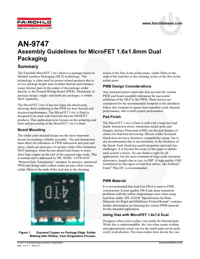
This document serves as an application note detailing the assembly guidelines for the Fairchild MicroFET 1.6x1.6mm Dual package. It focuses on soldering and back-end processing, emphasizing the importance of board mounting, pad design, and stencil optimization for reliable manufacturing. The package utilizes Molded Leadless Packaging (MLP) technology, featuring large die-attach pads for direct soldering to the Printed Wiring Board (PWB) to ensure optimal thermal and electrical performance.
Key topics include recommendations for PWB materials, specifically lead-free FR-4, and suitable pad finishes such as OSP, immersion silver, or immersion nickel gold. The note discusses the use of vias, voiding criteria (suggesting a maximum of 25% macro voiding), and rework procedures. It also outlines board-level reliability testing standards, noting that the package should withstand 1000 temperature cycles between -40°C and 125°C without failure.
| Package Type | MicroFET 1.6x1.6mm Dual |
|---|---|
| Technology | Molded Leadless Packaging (MLP) |
| Lead Finish | NiPdAu |
| Recommended Solder Alloy | SAC 305 |
| Maximum Voiding | 25% |
| Temperature Cycling Range | -40°C to 125°C |
| Temperature Cycling Cycles | 1000 |
| Peak Reflow Temperature | 260°C |
Fairchild suggests a maximum of 25% voiding for MLP type packages based on reliability studies.
It is recommended that this component not be reused if rework becomes necessary due to high temperatures associated with lead-free reflow.
The lead-free alloy SAC 305 is recommended as the choice for the electronics industry.
No, a solder fillet is not required on the side of the lead, but it can improve reliability by 20%.