
This document introduces the features and characteristics of Fairchild MicroFET™ package, including small size, low weight, thin base and good thermal and electrical performance.
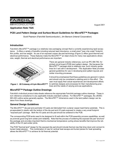
This document provides general guidelines for developing land pattern layouts and solder mounting processes for Fairchild's MicroFET package. It emphasizes that these guidelines are a starting point and should be optimized based on specific manufacturing practices and end-use application needs. The note references the JEDEC MO-220 outline series for package dimensions.
| Recommended Solder Paste Type | No Clean Type 3 paste per ANSI/J-STD-005 |
|---|---|
| Recommended Stencil Thickness (>0.5mm pitch) | 0.15mm to 0.2mm |
| Thermal Via Diameter | 0.3mm to 0.33mm |
| Thermal Via Copper Barrel | 1.0 ounce copper |
| Recommended Solder Mask Type | Non-Solder Mask Defined (NSMD) |
| Solder Mask Diameter for Thermal Vias | 100um larger than via diameter |
| Recommended Stencil Wall Type | Electropolished trapezoidal walls |
| Recommended Stencil Material | Laser-cut, stainless steel |
| Reflow Profile Peak Temperature | 240 F |
| Reflow Profile Cooling Rate | 1.3 TO 1.6 C/s |
| Pre-rework Bake Temperature | 125C |
| Pre-rework Bake Duration | at least 4 hours |
"No Clean Type 3 paste per ANSI/J-STD-005 is recommended."
NSMD (Non-Solder Mask Defined) is recommended for the perimeter I/O lands and generally for the thermal land.