
This application note focuses on the soldering and back end processing of the MicroFET 2x2
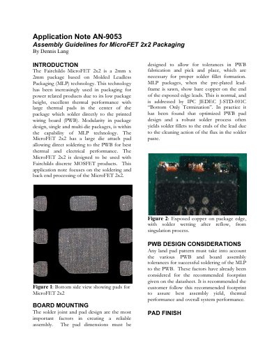
This application note details the assembly guidelines for the Fairchild MicroFET 2x2 package, a 2mm x 2mm Molded Leadless Packaging (MLP) device. It focuses on soldering and back-end processing to ensure reliable assembly and optimal thermal performance. The document addresses PWB design considerations, including pad finishes and the use of vias, as well as stencil design and solder paste selection.
| Package Dimensions | 2mm x 2mm |
|---|---|
| Peak Reflow Temperature | 260°C |
| Recommended Solder Alloy | SAC 305 (96.5Sn/3.0Au/0.5Cu) |
| Recommended PWB Material | Lead free FR-4 |
| Recommended Via Drill Size | 0.3mm |
| Recommended Stencil Thickness | 4 mils |
| Maximum Recommended Voiding | 25% |
The recommended lead-free solder paste alloy is SAC 305 (96.5Sn/3.0Au/0.5Cu).
Yes, but filled vias are preferred for high reliability applications to reduce voiding. Blind vias are not recommended.
Fairchild recommends a guideline of 25% maximum voiding for MLP type packages.
No, it is recommended that this component not be reused if rework becomes necessary due to high temperatures.