
This application note describes assembly guidelines and recommendations for the MicroFET 2x2, including pre-assembly preparation, mounting methods, reflow soldering, and back-end processing.
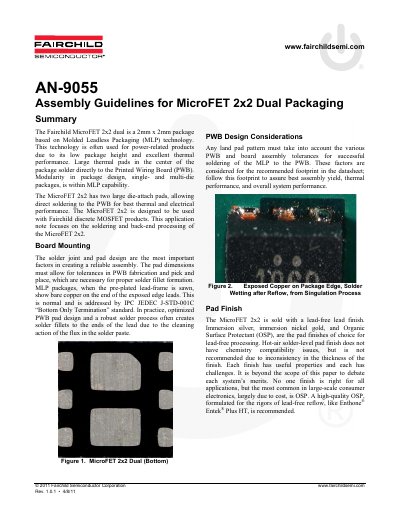
This application note provides assembly guidelines for the Fairchild MicroFET 2x2 dual package, which is a 2mm x 2mm Molded Leadless Packaging (MLP) device. It focuses on soldering and back-end processing to ensure reliable performance in power-related applications.
| Package Dimensions | 2mm x 2mm |
|---|---|
| Peak Reflow Temperature | 260°C |
| Recommended Solder Alloy | SAC 305 |
| Maximum Voiding Limit | <25% |
Immersion silver, immersion nickel gold, and Organic Surface Protectant (OSP) are the choices of choice. A high-quality OSP like Enthone® Entek® Plus HT is recommended.
It is recommended to place vias just outside the pad to avoid voiding issues, as appropriately sized vias can be costly in production.
No, a solder fillet is not required on the side of the lead per JDC-STD-001D, but it can improve reliability by 20%.