
The NDS351N is Fairchild's N-Channel logic level enhancement mode power field effect transistor, using copper lead frame's proprietary package design, with superior thermal and electrical performance. High density cell design for extremely low RDS(ON). Exceptional on-resistance and maximum DC current capability. Compact industry standard SOT-23 surface mount package.
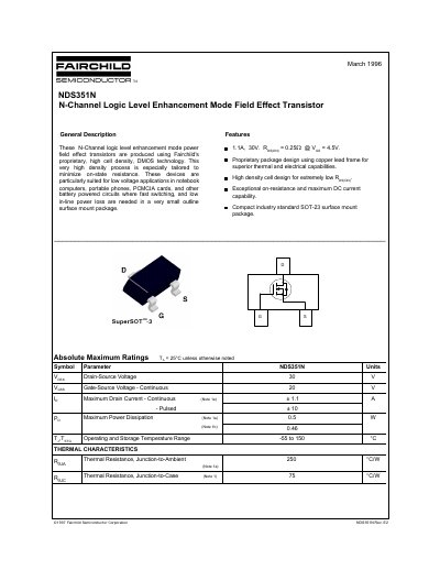
This document is a datasheet for the Fairchild Semiconductor NDS351N, an N-Channel logic level enhancement mode power field effect transistor. The device utilizes proprietary DMOS technology to minimize on-state resistance and is optimized for low voltage applications such as notebook computers, portable phones, and PCMCIA cards.
| Drain-Source Voltage | 30 V |
|---|---|
| Maximum Continuous Drain Current | +14 A |
| Maximum Power Dissipation | 0.5 W |
| Operating Temperature Range | -55 to 150 °C |
| Thermal Resistance Junction-to-Ambient | 250 °C/W |
The device supports a maximum continuous drain current of +14 A.
The maximum power dissipation is 0.5 W when mounted on a 0.02 in² pad of copper.