
This document introduces the dual P-Channel Enhancement Mode Power Field Effect Transistors produced by Fairchild Semiconductor Corporation. The product is produced using Fairchild's proprietary Trench Technology, which has a very high density and is designed to minimize on-state resistance, provide rugged and reliable performance, and fast switching speed. This product is particularly suitable for low voltage applications requiring a low current high side switch.
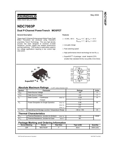
This document is a datasheet for the Fairchild Semiconductor NDC7003P, a dual P-channel enhancement mode PowerTrench MOSFET. The device is designed for low voltage applications requiring a low current high-side switch, featuring proprietary trench technology to minimize on-state resistance and provide fast switching speeds. It is available in the SuperSOT-6 package, which offers a small footprint and low profile.
The datasheet provides comprehensive electrical characteristics, including absolute maximum ratings, off and on characteristics, dynamic parameters, and switching characteristics. It also includes typical performance graphs such as on-resistance variation with temperature and gate charge characteristics, along with thermal response curves and maximum safe operating area diagrams.
| Drain-Source Voltage | -60 V |
|---|---|
| Gate-Source Voltage | +20 V |
| Continuous Drain Current | 0.34 A |
| Power Dissipation (Single Operation) | 0.96 W |
| Operating Temperature Range | -55 to +150 °C |
| Thermal Resistance (Junction-to-Ambient) | 130 °C/W |
| Package Type | SuperSOT-6 |
The maximum continuous drain current is 0.34 A.
The operating and storage junction temperature range is from -55 to +150 °C.
The device uses the SuperSOT-6 package, which has a small footprint and low profile.