
These devices are particularly suited for low voltage applications such as automotive, industrial, communication, and computer applications.
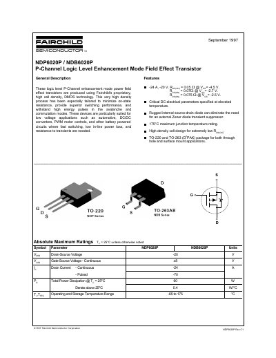
The document describes the Fairchild NDP6020P and NDB6020P, which are P-Channel Logic Level Enhancement Mode Field Effect Transistors produced using Fairchild's proprietary DMOS technology. These devices are designed for low voltage applications such as automotive systems, DC/DC converters, and PWM motor controls, offering fast switching and low in-line power loss.
| Drain-Source Voltage | -20 V |
|---|---|
| Gate-Source Voltage | ±8 V |
| Continuous Drain Current | -24 A |
| Total Power Dissipation | 60 W |
| Operating Temperature Range | -65 to 175 °C |
| On-Resistance (VGS=-4.5V) | 0.05 Ω |
| Thermal Resistance Junction-to-Case | 2.5 °C/W |
These devices are suited for low voltage applications such as automotive, DC/DC converters, PWM motor controls, and other battery powered circuits.
The maximum junction temperature rating is 175°C.
The device is available in TO-220 and TO-263 (D2 PAK) packages for both through hole and surface mount applications.