
This product is a P-channel logic level enhancement mode power field effect transistor with a rated current and voltage of -30 A and -30 V, extremely low RDS(ON) and a maximum junction temperature rating of 175°C.
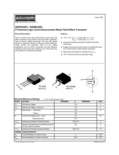
This document is a datasheet for the Fairchild NDP6030PL and NDB6030PL, which are P-Channel logic level enhancement mode power field effect transistors. Produced using Fairchild's proprietary high cell density DMOS technology, these devices are designed to minimize on-state resistance and are particularly suited for low voltage applications such as DC/DC converters and high efficiency switching circuits.
| Drain-Source Voltage | -30 V |
|---|---|
| Drain Current (Continuous) | -30 A |
| Total Power Dissipation | 75 W |
| Operating Temperature Range | -65 to 175 °C |
| Thermal Resistance (Junction-to-Case) | 2 °C/W |
| Static Drain-Source On-Resistance (Typical) | 0.042 Ω |
| Maximum Junction Temperature | 175°C |
The device features a rugged internal source-drain diode that can eliminate the need for an external Zener diode transient suppressor.
The maximum junction temperature rating is 175°C.
Yes, they are particularly suited for low voltage applications such as DC/DC converters and high efficiency switching circuits.