
This document introduces dual N and P-channel enhancement mode power field effect transistors produced by Fairchild Semiconductor. These transistors are made using the advanced PowerTrench process, which minimizes on-state resistance and maintains superior switching performance. They are suitable for low voltage and battery powered applications that require low in-line power loss and fast switching.
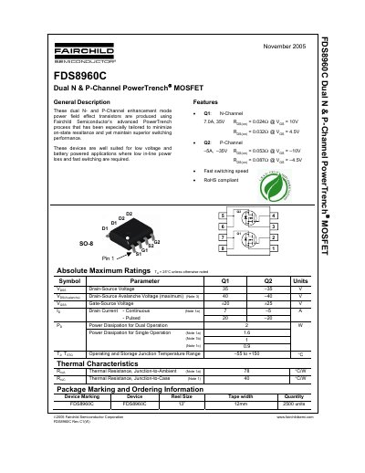
The Fairchild FDS8960C is a dual N- and P-Channel enhancement mode PowerTrench MOSFET designed using advanced manufacturing processes to minimize on-state resistance while maintaining superior switching performance. These devices are well suited for low voltage and battery powered applications where low in-line power loss and fast switching are required.
The document provides comprehensive electrical characteristics, including absolute maximum ratings, thermal data, and typical performance curves for both the N-Channel (Q1) and P-Channel (Q2) sections. Key features include a 35V drain-source voltage rating, low on-resistance values, RoHS compliance, and availability in an SSO-8 package.
| Drain-Source Voltage | +35 / -35 V |
|---|---|
| Power Dissipation (Dual Operation) | 2 W |
| Operating Junction Temperature Range | -55 to +150 °C |
The maximum continuous drain current is 7 A.
The operating and storage junction temperature range is from -55 to +150 °C.
The power dissipation for dual operation is 2 W.