
The FDS5690 is a 60V N-Channel PowerTrench MOSFET with low RDS(on) and fast switching speed. This device is well suited for low voltage and battery powered applications where low in-line power loss and fast switching are required.
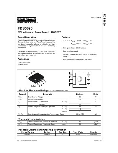
The document describes the Fairchild Semiconductor FDS5690, an N-Channel MOSFET produced using the advanced PowerTrench process. It is designed to minimize on-state resistance while maintaining superior switching performance, making it suitable for low voltage and battery-powered applications such as DC/DC converters and motor drives.
The datasheet details the device's absolute maximum ratings, including a 60V drain-source voltage and 7A continuous drain current. It also lists electrical characteristics like gate threshold voltage, on-resistance at various temperatures, capacitance values, and switching times. Typical performance is illustrated through graphs showing on-resistance variation with temperature and drain current, transfer characteristics, and safe operating areas.
| Drain-Source Voltage | 60 V |
|---|---|
| Gate-Source Voltage | +20 V |
| Continuous Drain Current | 7 A |
| Pulsed Drain Current | 50 A |
| Power Dissipation (Single Operation) | 2.5 W |
| Operating Junction Temperature Range | -55 to +150 °C |
| Thermal Resistance (Junction-to-Ambient) | 50 °C/W |
| Thermal Resistance (Junction-to-Case) | 25 °C/W |
| Total Gate Charge | 23 nC typical |
The device supports a continuous drain current of 7 A and a pulsed drain current of 50 A.
The MOSFET can operate and be stored within a junction temperature range of -55 to +150 °C.
The device can dissipate up to 2.5 W during single pulse operations.