
This document describes the features and characteristics of the dual N- and P-Channel enhancement mode power field effect transistors produced by Fairchild Semiconductor. These transistors are made using the PowerTrench process, which minimizes on-state resistance while maintaining superior switching performance. They are suitable for applications such as inverters and power supplies.
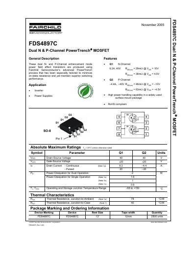
The FDS4897C is a dual N- and P-Channel enhancement mode power field effect transistor produced using Fairchild Semiconductors advanced PowerTrench process. It is designed to minimize on-state resistance while maintaining superior switching performance. The device is suitable for applications such as inverters and power supplies.
| Power Dissipation (Dual Operation) | 2 W |
|---|---|
| Operating Junction Temperature Range | -55 to +150 °C |
The N-Channel can handle 6.2 A, while the P-Channel handles 4.4 A continuously.
The device can dissipate a maximum of 2 W when both channels operate together.