
This document describes the features and absolute maximum ratings of the FDN337N N-Channel Logic Level Enhancement Mode Field Effect Transistor released in March 1998. The product features a high density cell design, extremely low on-resistance, and maximum DC current capability, making it suitable for low voltage applications where fast switching and low in-line power loss are required.
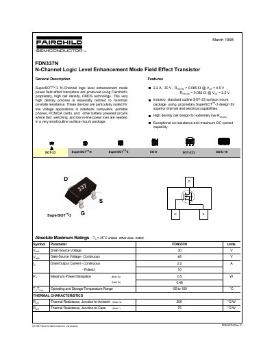
This document is a technical datasheet for the Fairchild Semiconductor FDN337N, an N-channel logic level enhancement mode power field effect transistor. The device utilizes proprietary SuperSOT™-3 design technology to minimize on-state resistance and is optimized for low voltage applications in battery-powered circuits such as notebook computers and portable phones.
The datasheet provides absolute maximum ratings, electrical characteristics, dynamic parameters, and switching specifications. It includes typical performance curves illustrating on-resistance variation with temperature and gate-to-source voltage, as well as safe operating area limits.
| Drain-Source Voltage (VSS) | 30 V |
|---|---|
| Gate-Source Voltage (Continuous) | +8 V |
| Maximum Power Dissipation | 0.5 W |
| Operating Temperature Range | -55 to 150 °C |
| Thermal Resistance (Junction-to-Ambient) | 250 °C/W |
The device uses an industry standard outline SOT-23 surface mount package with a proprietary SuperSOT™-3 design.
These devices are suited for low voltage applications in notebook computers, portable phones, PCMCIA cards, and other battery powered circuits.