
FDC6321C dual N & P channel digital FETs have very low gate drive requirements allowing direct operation in 3V circuits.
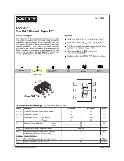
The document describes the Fairchild FDC6321C, which utilizes proprietary high cell density DMOS technology to minimize on-state resistance. It is specifically designed as a replacement for digital transistors in load switching applications where bias resistors are not required.
Key features include very low gate drive requirements allowing direct operation in 3 V circuits and integrated Gate-Source Zeners for ESD ruggedness (6kV Human Body Model). The device offers N-channel ratings of 25 V, 0.68 A, and P-channel ratings of -25 V, -0.46 A.
| N-Ch Drain-Source Voltage | 25 V |
|---|---|
| P-Ch Drain-Source Voltage | -25 V |
| N-Ch Continuous Drain Output Current | 0.68 A |
| P-Ch Continuous Drain Output Current | -0.46 A |
| N-Ch On-Resistance (Typ) | 0.45 Ω @ Vgs=4.5V |
| P-Ch On-Resistance (Typ) | 1.1 Ω @ Vgs=-4.5V |
| ESD Rating (Human Body Model) | >6kV |
It is designed especially for low voltage applications as a replacement for digital transistors in load switching applications.
No, since bias resistors are not required, the dual digital FET can replace several digital transistors with different bias resistors.
The typical gate threshold voltage is 0.8 V, with a minimum of 0.65 V.