
This document describes the features and characteristics of the FDD6N25 / FDU6N25 250V N-Channel MOSFET, including current, voltage, switching speed, and other parameters.
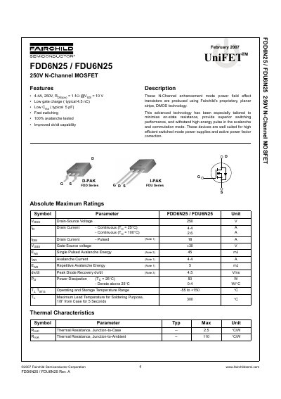
This datasheet describes the Fairchild Semiconductor FDD6N25 and FDU6N25, which are 250V N-Channel enhancement mode power field effect transistors. These devices utilize proprietary planar stripe, DMOS technology to minimize on-state resistance and provide superior switching performance. They are well suited for high efficient switched mode power supplies and active power factor correction applications.
| Drain-Source Voltage | 250 V |
|---|---|
| Continuous Drain Current (Tj = 25°C) | 4.4 A |
| Pulsed Drain Current | 18 A |
| Total Gate Charge | 4.5 nC |
| Reverse Transfer Capacitance | 5 pF |
| Power Dissipation (Tj = 25°C) | 50 W |
| Operating Temperature Range | -55 to +150 °C |
| Package Types | D-PAK, I-PAK |
These devices are well suited for high efficient switched mode power supplies and active power factor correction.
The maximum junction temperature is 150 °C.
The typical gate charge is 4.5 nC.