
The FDC6327C is a dual N and P channel 2.5V specified PowerTrench™ MOSFET. It is manufactured using Fairchild Semiconductor's advanced PowerTrench process that has been specially tailored to minimize on-state resistance and yet maintain low gate charge for superior switching performance. These devices have been designed to offer exceptional power dissipation in a very small footprint for applications where the bigger more expensive SO-8 and TSSOP-8 packages are impractical.
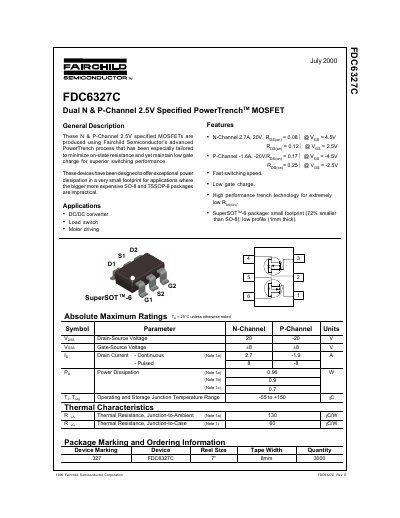
The document describes the Fairchild Semiconductor FDC6327C, which utilizes advanced PowerTrench technology to minimize on-state resistance while maintaining low gate charge. The device is designed for applications requiring high power dissipation in a small footprint, such as DC/DC converters, load switches, and motor drivers.
The datasheet provides comprehensive electrical characteristics, including absolute maximum ratings, thermal specifications, and typical performance curves for both N-channel (2.7A, 20V) and P-channel (-1.6A, -20V) sections. It also includes information on the SuperSOT-6 package dimensions and ordering details.
| Drain-Source Voltage (N-Channel) | 20 V |
|---|---|
| Drain Current (Continuous, P-Channel) | -1.6 A |
| Package Type | SuperSOT™-6 |
| Operating Junction Temperature Range | -55 to +150 °C |
The device is designed for DC/DC converters, load switches, and motor drivers.
The typical on-state resistance (RDS(on)) for the N-Channel is 0.082 Ohms.