
The DS90CF383B is a programmable LVDS transmitter that converts 28 bits of CMOS/TTL data into four LVDS data streams. It supports a transmit clock frequency of 65 MHz and can transmit 24 bits of RGB data and 3 bits of LCD timing and control data at a rate of 455 Mbps per LVDS data channel. The DS90CF383B is fixed as a Falling edge strobe transmitter and will interoperate with a Falling edge strobe Receiver (DS90CF386) without any translation logic. This chipset is an ideal means to solve EMI and cable size problems associated with wide, high speed TTL interfaces.
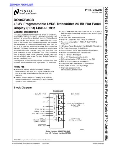
The DS90CF383B is a +3.3V Programmable LVDS Transmitter designed to convert 28 bits of CMOS/TTL data into four LVDS data streams and one transmit clock stream. It supports up to 65 MHz shift clocks, enabling data throughput of up to 227 Mbytes/sec for applications such as VGA, SVGA, XGA, and SXGA displays.
| Supply Voltage (Vcc) | 3.0 V to 3.6 V |
|---|---|
| Operating Temperature Range | -10°C to +70°C |
| Maximum Package Power Dissipation | 1.63 W |
| LVDS Differential Output Voltage (Typical) | 345 mV |
| Data Throughput (Typical) | Up to 227 Mbytes/sec |
The DS90CF383B supports a shift clock range from 18 to 68 MHz.
The recommended operating supply voltage is 3.3V.
Power consumption drops to less than 60 microWatts in typical conditions during power-down.