
The DS90C387A/DS90CF388A transmitter/receiver pair is designed to support dual pixel data transmission between Host and Flat Panel Display up to QXGA resolutions. The transmitter converts 48 bits (Dual Pixel 24-bit color) of CMOS/TTL data and 3 control bits into 8 LVDS (Low Voltage Differential Signalling) data streams. At a maximum dual pixel rate of 112MHz, LVDS data line speed is 784Mbps, providing a total throughput of 5.7Gbps (714 Megabytes per second). The LDI chipset is improved over prior generations of FPD-Link devices and offers higher bandwidth support and longer cable drive. To increase bandwidth, the maximum pixel clock rate is increased to 112 MHz and 8 serialized LVDS outputs are provided. Cable drive is enhanced with a user selectable pre-emphasis feature that provides additional output current during transitions to counteract cable loading effects. The DS90C387A transmitter provides a second LVDS output clock. Both LVDS clocks are identical. This feature supports backward compatibility with the previous generation of FPD-Link Receivers - the second clock allows the transmitter to interface to panels using a 'dual pixel' configuration of two 24-bit or 18-bit FPD-Link receivers. This chipset is an ideal means to solve EMI and cable size problems for high-resolution flat panel applications.
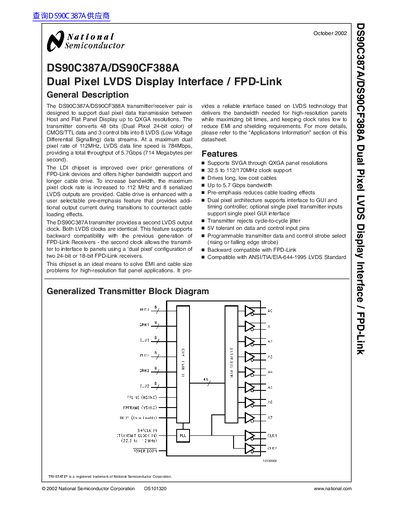
The DS90C387A/DS90CF388A chipset is a transmitter/receiver pair designed to support dual pixel data transmission between a host and a flat panel display up to QXGA resolutions. The transmitter converts 48 bits of CMOS/TTL data and 3 control bits into 8 LVDS data streams, achieving a maximum dual pixel rate of 112MHz and a total throughput of 5.7Gbps. This chipset offers higher bandwidth support and longer cable drive compared to prior generations of FPD-Link devices.
| Maximum Dual Pixel Rate | 112MHz |
|---|---|
| Total Throughput | 5.7Gbps |
| Junction Temperature | +150°C |
| Bandwidth | Up to 5.7 Gbps |
The chipset supports SVGA through QXGA panel resolutions.
The maximum pixel clock rate is increased to 112 MHz.
Yes, it is backward compatible with the previous generation of FPD-Link Receivers.