
The IDT54/74FCT377T/AT/CT/DT are octal D flip-flops built using an advanced dual metal CMOS technology. They have eight edge-triggered, D-type flip-flops with individual D inputs and O outputs. The common buffered Clock (CP) input loads all flip-flops simultaneously when the Clock Enable (CE) is LOW. The register is fully edge-triggered. The state of each D input, one set-up time before the LOW-to-HIGH clock transition, is transferred to the corresponding flip-flop’s O output. The CE input must be stable only one set-up time prior to the LOW-to-HIGH transi- tion for predictable operation.
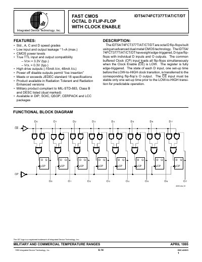
The IDT54/74FCT377T/AT/CT/DT is an octal D‑type flip‑flop built with advanced dual‑metal CMOS technology. It features individual D inputs, O outputs, a common buffered clock, and a Clock Enable (CE) pin that is active low, allowing simultaneous loading of all flip‑flops.
The document lists detailed electrical characteristics, absolute maximum ratings, power‑supply requirements, switching characteristics, test circuits, and ordering information. It also specifies available speed grades, package types, and temperature ranges for both commercial and military versions.
| Input leakage | ≤1 µA (max) |
|---|---|
| Output high‑drive current | -15 mA I_OH |
| Speed grades | Std., A, C, D |
| Commercial operating temperature | 0 °C to +70 °C |
| Military operating temperature | –55 °C to +125 °C |
CE is active low; when CE is LOW the common buffered clock loads all flip‑flops simultaneously.
The device is offered in DIP, SOIC, QSOP, CERPACK, and LCC packages.