
PSD4235G2V is an integrated solution provided by PSD, including configurable memories, PLD logic and I/O, suitable for applications based on 16-bit MCU. It has dual-port flash memory, PLD macrocells, 7 I/O ports, In-System Programming (ISP) and JTAG.
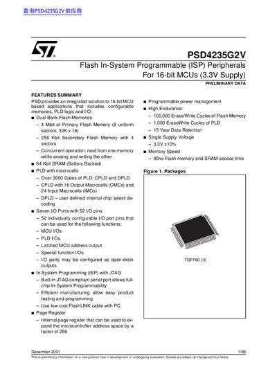
This manual describes the PSD4235G2V flash‑in‑system programmable peripheral, including its dual‑bank flash memories, battery‑backed SRAM, and programmable logic blocks. It outlines the architecture, pin assignments, power‑management features, and the JTAG‑based programming interface.
The document also covers In‑System Programming (ISP) via JTAG, In‑Application Programming (IAP) using the dual flash banks, and detailed register descriptions, timing tables, and development tools such as PSDsoft Express.
| Primary Flash Memory | 4 Mbit (8 sectors, 32K x 16) |
|---|---|
| Secondary Flash Memory | 256 Kbit (4 sectors) |
| SRAM | 64 Kbit battery‑backed |
| PLD Gate Count | over 3000 gates |
| CPLD Macrocell Count | 16 Output, 24 Input |
| I/O Pins | 52 individually configurable pins |
| Supply Voltage | 3.38 V ±10% |
| Memory Access Time | 90 ns |
| Flash Endurance | 100,000 erase/write cycles |
| PLD Endurance | 1,000 erase/write cycles |
| Data Retention | 15 years |
The secondary Flash memory can be used to execute code while the primary Flash is being erased or programmed, enabling concurrent read/write operations during In‑Application Programming (IAP).
It operates from a single 3.38 V supply with a ±10 % tolerance.
The PSD4235G2V provides 52 individually configurable I/O pins distributed across seven ports.