
STW7NA80 and STH7NA80FI are N-channel enhancement mode fast power MOS transistors with low intrinsic capacitances, minimized gate charge, and reduced threshold voltage spread. They are suitable for high current, high-speed switching, switch mode power supplies (SMPS), DC-AC converters for welding equipment and uninterruptible power supplies, and motor drive.
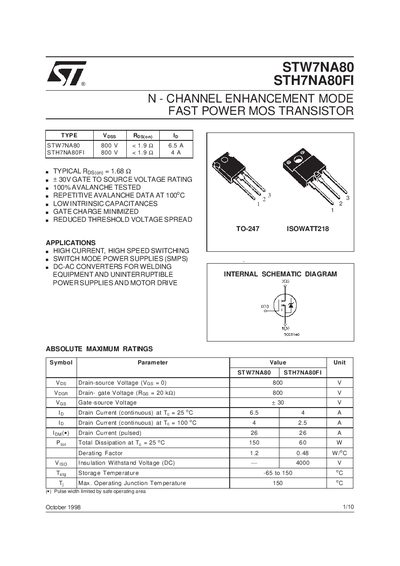
This handbook provides the electrical, thermal and mechanical specifications for the STW7NA80 and STH7NA80FI N‑channel fast power MOSFETs manufactured by STMicroelectronics. It includes typical characteristics, maximum ratings, avalanche data, switching performance and package dimensions.
The document also contains application notes such as high‑current, high‑speed switching for SMPS, DC‑AC converters for welding equipment, UPS and motor drives, together with detailed test circuit diagrams and derating curves.
| Drain‑source Voltage | 800 V |
|---|---|
| Gate‑source Voltage Rating | +30 V |
| Continuous Drain Current (STW7NA80) | 6.5 A |
| Pulsed Drain Current | 26 A |
| Total Dissipation (STW7NA80) | 150 W |
| Total Dissipation (STH7NA80FI) | 60 W |
| Insulation Withstand Voltage | 4000 V |
| Maximum Junction Temperature | 150 °C |
| Thermal Resistance Junction‑case (STW7NA80) | 0.83 °C/W |
| Thermal Resistance Junction‑case (STH7NA80FI) | 2.08 °C/W |
| Avalanche Current | 6.3 A |
The MOSFETs are rated for a maximum drain‑source voltage of 800 V.
The gate‑to‑source voltage rating is +30 V.
STW7NA80 can handle 6.5 A continuous drain current, while STH7NA80FI is rated at 4 A.
The maximum junction temperature is 150 °C.