
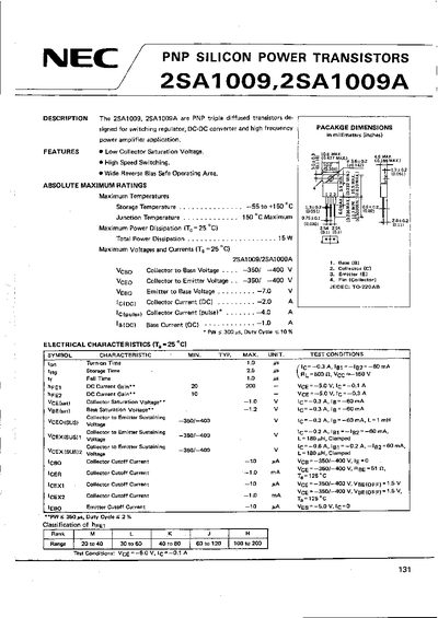
The 2SA1009 and 2SA1009A are PNP triple‑diffused silicon power transistors intended for switching regulators, DC‑DC converters, and high‑frequency power‑amplifier applications. The document lists their absolute maximum ratings, electrical characteristics, and typical performance curves.
Key specifications include collector‑to‑base and collector‑to‑emitter voltage limits of 350‑400 V, a maximum continuous collector current of 2 A (4 A pulsed), and a power dissipation capability of up to 15 W at a case temperature of 25 °C. Thermal resistance, current gain, and safe operating area curves are also provided.
| Collector to Base Voltage | ‑350 V to ‑400 V |
|---|---|
| Collector to Emitter Voltage | ‑350 V to ‑400 V |
| Collector Current (DC) | ‑2.0 A |
| Collector Current (pulse) | ‑4.0 A |
| Base Current (DC) | ‑1.0 A |
| Maximum Junction Temperature | 150 °C |
| DC Current Gain (hFE) typical | 20 – 200 (VCE=5 V) |
The device can withstand a collector‑to‑emitter voltage of 350 V to 400 V.
The maximum junction temperature is rated at 150 °C.