
NE650R479A is a 0.4 W GaAs MES FET designed for middle power transmitter applications for mobile communication handset and base station systems. It is capable of delivering 0.4 watt of output power (CW) with high linear gain, high efficiency, excellent distortion and is suitable as a driver amplifier for our NE6500379A etc. Reliability and performance uniformity are assured by NEC’s stringent quality and control procedures.
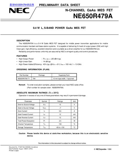
The NE650R479A is a 0.4 W N‑channel GaAs MES FET intended for middle‑power transmitter applications in mobile handsets and base stations. The datasheet provides absolute maximum ratings, recommended operating limits, electrical characteristics, S‑parameters, package dimensions and soldering guidelines.
Key sections cover device features, ordering information, absolute maximum ratings, electrical characteristics, application circuit examples and recommended soldering conditions, helping designers assess suitability and integrate the component safely.
| Output Power (1 dB compression) | 26.0 dBm typ |
|---|---|
| Linear Gain | 14 dB typ |
| Power Added Efficiency | 45 % typ |
| Drain‑to‑Source Voltage (VDS) | 15 V max |
| Gate‑to‑Source Voltage (VGS0) | –7 V max |
| Drain Current (ID) | 0.6 A max |
| Total Power Dissipation (PT) | 2.5 W max |
| Channel Temperature (Tch) | 150 °C max |
| Recommended VDS (operation) | 6.0 V |
| Recommended Gain Compression | 3.0 dB |
The device can handle up to 0.6 A of drain current.
Infrared reflow: peak temperature ≤ 235 °C, time ≤ 30 s at 210 °C, two exposures; partial heating: pin temperature ≤ 260 °C, time ≤ 5 s per pin row.
Typical output power is 26 dBm at the 1 dB compression point.
The recommended VDS for normal operation is 6 V.