
MC74VHC1G135 is a single gate MOS open drain output trigger fabricated with silicon gate CMOS technology produced by LESHAN RADIO COMPANY, LTD.
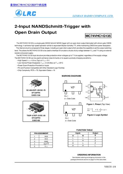
The MC74VHC1G135 is a single‑gate CMOS Schmitt‑trigger NAND device with an open‑drain output, designed for high‑speed operation while maintaining low power dissipation. It can interface 5 V circuits to voltages up to 7 V using an external resistor and power supply.
Key specifications include a typical propagation delay of 4.9 ns at 5 V, supply voltage range of –0.5 V to +7 V, and a maximum output current of 25 mA per pin. Ordering information, pin assignments, and electrical characteristics are detailed for various package types (SC‑70, SC‑88A, SOT‑23, etc.).
| Propagation delay (t_pp) typ | 4.9 ns at Vcc=5 V |
|---|---|
| DC supply voltage range | -0.5 V to +7.0 V |
| Operating temperature range | -55 °C to +125 °C |
| Maximum output current per pin | 25 mA |
The typical propagation delay is 4.9 ns when Vcc is 5 V.
It can operate from –0.5 V up to +7.0 V.
Each output pin can source up to 25 mA.